
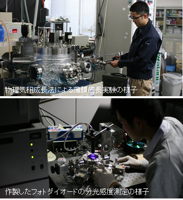
We conduct research on sensing materials and devices, as well as the processes and evaluation technologies required for device fabrication, encompassing elemental technologies from material creation to evaluation and device fabrication. For the creation of sensing materials, we primarily employ physical vapor deposition methods such as sputtering and coaxial arc plasma deposition. Recently, with the aim of creating IoT devices capable of operating in extreme environments such as outer space, we have been focusing on the creation of all-diamond optical, magnetic, and chemical sensing devices.
Member
The Main Research Topics
Development of all-diamond optical, magnetic, and chemical sensing devices capable of operating in extreme environments, including outer space
Fabrication of pn-junction-type photodetectors based on heteroepitaxial growth of gallium oxide films on diamond substrates
Process development for nanodiamond film growth by physical vapor deposition and its applications to hard coatings and bioaffinity coatings